Journals > > Topics > Integrated Optics
Integrated Optics|114 Article(s)
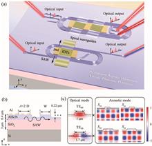
Demonstration of acousto-optical modulation based on a thin-film AlScN photonic platform
Kewei Bian, Zhenyu Li, Yushuai Liu, Sumei Xu, Xingyan Zhao, Yang Qiu, Yuan Dong, Qize Zhong, Tao Wu, Shaonan Zheng, and Ting Hu
Acousto-optic (AO) modulation technology holds significant promise for applications in microwave and optical signal processing. Thin-film scandium-doped aluminum nitride (AlScN), with excellent piezoelectric properties and a wide transparency window, is a promising candidate for achieving on-chip AO modulation with a fabrication process compatible with complementary metal-oxide-semiconductor (CMOS) technology. This study presents, to the best of our knowledge, the first demonstration of AO modulators with surface acoustic wave generation and photonic waveguides monolithically integrated on a 400-nm-thick film of AlScN on an insulator. The intramodal AO modulation is realized based on an AlScN straight waveguide, and the modulation efficiency is significantly enhanced by 12.3 dB through the extension of the AO interaction length and the utilization of bidirectional acoustic energy. The intermodal AO modulation and non-reciprocity are further demonstrated based on a multi-mode spiral waveguide, achieving a high non-reciprocal contrast (>10 dB) across an optical bandwidth of 0.48 nm. This research marks a significant stride forward, representing an advancement in the realization of microwave photonic filters, magnet-free isolators, and circulators based on the thin-film AlScN photonic platform. Acousto-optic (AO) modulation technology holds significant promise for applications in microwave and optical signal processing. Thin-film scandium-doped aluminum nitride (AlScN), with excellent piezoelectric properties and a wide transparency window, is a promising candidate for achieving on-chip AO modulation with a fabrication process compatible with complementary metal-oxide-semiconductor (CMOS) technology. This study presents, to the best of our knowledge, the first demonstration of AO modulators with surface acoustic wave generation and photonic waveguides monolithically integrated on a 400-nm-thick film of AlScN on an insulator. The intramodal AO modulation is realized based on an AlScN straight waveguide, and the modulation efficiency is significantly enhanced by 12.3 dB through the extension of the AO interaction length and the utilization of bidirectional acoustic energy. The intermodal AO modulation and non-reciprocity are further demonstrated based on a multi-mode spiral waveguide, achieving a high non-reciprocal contrast (>10 dB) across an optical bandwidth of 0.48 nm. This research marks a significant stride forward, representing an advancement in the realization of microwave photonic filters, magnet-free isolators, and circulators based on the thin-film AlScN photonic platform.
Photonics Research
- Publication Date: May. 17, 2024
- Vol. 12, Issue 6, 1138 (2024)


Highly efficient fiber to Si waveguide free-form coupler for foundry-scale silicon photonics|Editors' Pick
Luigi Ranno, Jia Xu Brian Sia, Cosmin Popescu, Drew Weninger, Samuel Serna, Shaoliang Yu, Lionel C. Kimerling, Anuradha Agarwal, Tian Gu, and Juejun Hu
As silicon photonics transitions from research to commercial deployment, packaging solutions that efficiently couple light into highly compact and functional sub-micrometer silicon waveguides are imperative but remain challenging. The 220 nm silicon-on-insulator (SOI) platform, poised to enable large-scale integration, is the most widely adopted by foundries, resulting in established fabrication processes and extensive photonic component libraries. The development of a highly efficient, scalable, and broadband coupling scheme for this platform is therefore of paramount importance. Leveraging two-photon polymerization (TPP) and a deterministic free-form micro-optics design methodology based on the Fermat’s principle, this work demonstrates an ultra-efficient and broadband 3-D coupler interface between standard SMF-28 single-mode fibers and silicon waveguides on the 220 nm SOI platform. The coupler achieves a low coupling loss of 0.8 dB for the fundamental TE mode, along with 1 dB bandwidth exceeding 180 nm. The broadband operation enables diverse bandwidth-driven applications ranging from communications to spectroscopy. Furthermore, the 3-D free-form coupler also enables large tolerance to fiber misalignments and manufacturing variability, thereby relaxing packaging requirements toward cost reduction capitalizing on standard electronic packaging process flows. As silicon photonics transitions from research to commercial deployment, packaging solutions that efficiently couple light into highly compact and functional sub-micrometer silicon waveguides are imperative but remain challenging. The 220 nm silicon-on-insulator (SOI) platform, poised to enable large-scale integration, is the most widely adopted by foundries, resulting in established fabrication processes and extensive photonic component libraries. The development of a highly efficient, scalable, and broadband coupling scheme for this platform is therefore of paramount importance. Leveraging two-photon polymerization (TPP) and a deterministic free-form micro-optics design methodology based on the Fermat’s principle, this work demonstrates an ultra-efficient and broadband 3-D coupler interface between standard SMF-28 single-mode fibers and silicon waveguides on the 220 nm SOI platform. The coupler achieves a low coupling loss of 0.8 dB for the fundamental TE mode, along with 1 dB bandwidth exceeding 180 nm. The broadband operation enables diverse bandwidth-driven applications ranging from communications to spectroscopy. Furthermore, the 3-D free-form coupler also enables large tolerance to fiber misalignments and manufacturing variability, thereby relaxing packaging requirements toward cost reduction capitalizing on standard electronic packaging process flows.
Photonics Research
- Publication Date: May. 01, 2024
- Vol. 12, Issue 5, 1055 (2024)

Time-space multiplexed photonic-electronic digital multiplier
Wenkai Zhang, Bo Wu, Wentao Gu, Junwei Cheng, Hailong Zhou, Liao Chen, Wenchan Dong, Jianji Dong, and Xinliang Zhang
Optical computing has shown immense application prospects in the post-Moore era. However, as a crucial component of logic computing, the digital multiplier can only be realized on a small scale in optics, restrained by the limited functionalities and inevitable loss of optical nonlinearity. In this paper, we propose a time-space multiplexed architecture to realize large-scale photonic-electronic digital multiplication. We experimentally demonstrate an 8×2-bit photonic-electronic digital multiplier, and the multiplication with a 32-bit number is further executed at 25 Mbit/s to demonstrate its extensibility and functionality. Moreover, the proposed architecture has the potential for on-chip implementation, and a feasible integration scheme is provided. We believe the time-space multiplexed photonic-electronic digital multiplier will open up a promising avenue for large-scale photonic digital computing. Optical computing has shown immense application prospects in the post-Moore era. However, as a crucial component of logic computing, the digital multiplier can only be realized on a small scale in optics, restrained by the limited functionalities and inevitable loss of optical nonlinearity. In this paper, we propose a time-space multiplexed architecture to realize large-scale photonic-electronic digital multiplication. We experimentally demonstrate an 8×2-bit photonic-electronic digital multiplier, and the multiplication with a 32-bit number is further executed at 25 Mbit/s to demonstrate its extensibility and functionality. Moreover, the proposed architecture has the potential for on-chip implementation, and a feasible integration scheme is provided. We believe the time-space multiplexed photonic-electronic digital multiplier will open up a promising avenue for large-scale photonic digital computing.
Photonics Research
- Publication Date: Mar. 01, 2024
- Vol. 12, Issue 3, 499 (2024)

Silicon photonic integrated interrogator for fiber-optic distributed acoustic sensing
Zhicheng Jin, Jiageng Chen, Yanming Chang, Qingwen Liu, and Zuyuan He
Distributed acoustic sensing (DAS) technology has been a promising tool in various applications. Currently, the large size and relatively high cost of DAS equipment composed of discrete devices restrict its further popularization to some degree, and the photonic integration technology offers a potential solution. In this paper, we demonstrate an integrated interrogator for DAS on the silicon-on-insulator (SOI) platform. The design of the chip revolves around a Mach–Zehnder modulator (MZM) transmitter and a dual-quadrature and dual-polarization coherent receiver. The integrated interrogator supports multiple DAS schemes, including the time-gated digital optical frequency domain reflectometry (TGD-OFDR), which is adopted for system performance evaluation. 59 pε/Hz strain resolution in 12.1 km sensing fiber with 1.14 m spatial resolution (SR) is realized. Besides, along 49.0 km sensing fiber, 81 pε/Hz strain resolution with 3.78 m SR is achieved. The results show that the integrated interrogator has comparable performance to the discrete DAS system. To the best of our knowledge, this is the first dedicated on-chip DAS interrogator, which validates the effectiveness of the blend of photonics integration and DAS technology. Distributed acoustic sensing (DAS) technology has been a promising tool in various applications. Currently, the large size and relatively high cost of DAS equipment composed of discrete devices restrict its further popularization to some degree, and the photonic integration technology offers a potential solution. In this paper, we demonstrate an integrated interrogator for DAS on the silicon-on-insulator (SOI) platform. The design of the chip revolves around a Mach–Zehnder modulator (MZM) transmitter and a dual-quadrature and dual-polarization coherent receiver. The integrated interrogator supports multiple DAS schemes, including the time-gated digital optical frequency domain reflectometry (TGD-OFDR), which is adopted for system performance evaluation. 59 pε/Hz strain resolution in 12.1 km sensing fiber with 1.14 m spatial resolution (SR) is realized. Besides, along 49.0 km sensing fiber, 81 pε/Hz strain resolution with 3.78 m SR is achieved. The results show that the integrated interrogator has comparable performance to the discrete DAS system. To the best of our knowledge, this is the first dedicated on-chip DAS interrogator, which validates the effectiveness of the blend of photonics integration and DAS technology.
Photonics Research
- Publication Date: Feb. 26, 2024
- Vol. 12, Issue 3, 465 (2024)

Chiral forces in longitudinally invariant dielectric photonic waveguides
Josep Martínez-Romeu, Iago Diez, Sebastian Golat, Francisco J. Rodríguez-Fortuño, and Alejandro Martínez
We calculate numerically the optical chiral forces in rectangular cross-section dielectric waveguides for potential enantiomer separation. Our study considers force strength and time needed for separating chiral nanoparticles, mainly via quasi-TE guided modes at short wavelengths (405 nm) and the 90°-phase-shifted combination of quasi-TE and quasi-TM modes at longer wavelengths (1310 nm). Particle tracking simulations show successful enantiomer separation within two seconds. These results suggest the feasibility of enantiomeric separation of nanoparticles displaying sufficient chirality using simple silicon photonic integrated circuits, with wavelength selection based on the nanoparticle size. We calculate numerically the optical chiral forces in rectangular cross-section dielectric waveguides for potential enantiomer separation. Our study considers force strength and time needed for separating chiral nanoparticles, mainly via quasi-TE guided modes at short wavelengths (405 nm) and the 90°-phase-shifted combination of quasi-TE and quasi-TM modes at longer wavelengths (1310 nm). Particle tracking simulations show successful enantiomer separation within two seconds. These results suggest the feasibility of enantiomeric separation of nanoparticles displaying sufficient chirality using simple silicon photonic integrated circuits, with wavelength selection based on the nanoparticle size.
Photonics Research
- Publication Date: Feb. 26, 2024
- Vol. 12, Issue 3, 431 (2024)

Mode-insensitive and mode-selective optical switch based on asymmetric Y-junctions and MMI couplers
Shijie Sun, Qidong Yu, Yuanhua Che, Tianhang Lian, Yuhang Xie, Daming Zhang, and Xibin Wang
Driven by the large volume demands of data in transmission systems, the number of spatial modes supported by mode-division multiplexing (MDM) systems is being increased to take full advantage of the parallelism of the signals in different spatial modes. As a key element for photonic integrated circuits, the multimode waveguide optical switch (MWOS) is playing an important role for data exchange and signal switching. However, the function of the traditional MWOS is simple, which could only implement the mode-insensitive or mode-selective switching function; it is also difficult to scale to accommodate more spatial modes because of the limitation of the device structure. Therefore, it is still challenging to realize a multifunctional and scalable MWOS that could support multiple modes with low power consumption and high flexibility. Here, we propose and experimentally demonstrate a multifunctional MWOS based on asymmetric Y-junctions and multimode interference (MMI) couplers fabricated on a polymer waveguide platform. Both mode-insensitive and mode-selective switching functions can be achieved via selectively heating different electrode heaters. The fabricated device with the total length of ∼0.8 cm shows an insertion loss of less than 12.1 dB, and an extinction ratio of larger than 8.4 dB with a power consumption of ∼32 mW for both mode-insensitive and mode-selective switching functions, at 1550 nm wavelength. The proposed MWOS can also be scaled to accommodate more spatial modes flexibly and easily, which can serve as an important building block for MDM systems. Driven by the large volume demands of data in transmission systems, the number of spatial modes supported by mode-division multiplexing (MDM) systems is being increased to take full advantage of the parallelism of the signals in different spatial modes. As a key element for photonic integrated circuits, the multimode waveguide optical switch (MWOS) is playing an important role for data exchange and signal switching. However, the function of the traditional MWOS is simple, which could only implement the mode-insensitive or mode-selective switching function; it is also difficult to scale to accommodate more spatial modes because of the limitation of the device structure. Therefore, it is still challenging to realize a multifunctional and scalable MWOS that could support multiple modes with low power consumption and high flexibility. Here, we propose and experimentally demonstrate a multifunctional MWOS based on asymmetric Y-junctions and multimode interference (MMI) couplers fabricated on a polymer waveguide platform. Both mode-insensitive and mode-selective switching functions can be achieved via selectively heating different electrode heaters. The fabricated device with the total length of ∼0.8 cm shows an insertion loss of less than 12.1 dB, and an extinction ratio of larger than 8.4 dB with a power consumption of ∼32 mW for both mode-insensitive and mode-selective switching functions, at 1550 nm wavelength. The proposed MWOS can also be scaled to accommodate more spatial modes flexibly and easily, which can serve as an important building block for MDM systems.
Photonics Research
- Publication Date: Feb. 08, 2024
- Vol. 12, Issue 3, 423 (2024)
Scalable orthogonal delay-division multiplexed OEO artificial neural network trained for TI-ADC equalization
Andrea Zazzi, Arka Dipta Das, Lukas Hüssen, Renato Negra, and Jeremy Witzens
We propose a new signaling scheme for on-chip optical-electrical-optical artificial neural networks that utilizes orthogonal delay-division multiplexing and pilot-tone-based self-homodyne detection. This scheme offers a more efficient scaling of the optical power budget with increasing network complexity. Our simulations, based on 220 nm silicon-on-insulator silicon photonics technology, suggest that the network can support 31×31 neurons, with 961 links and freely programmable weights, using a single 500 mW optical comb and a signal-to-noise ratio of 21.3 dB per neuron. Moreover, it features a low sensitivity to temperature fluctuations, ensuring that it can be operated outside of a laboratory environment. We demonstrate the network’s effectiveness in nonlinear equalization tasks by training it to equalize a time-interleaved analog-to-digital converter (ADC) architecture, achieving an effective number of bits over 4 over the entire 75 GHz ADC bandwidth. We anticipate that this network architecture will enable broadband and low latency nonlinear signal processing in practical settings such as ultra-broadband data converters and real-time control systems. We propose a new signaling scheme for on-chip optical-electrical-optical artificial neural networks that utilizes orthogonal delay-division multiplexing and pilot-tone-based self-homodyne detection. This scheme offers a more efficient scaling of the optical power budget with increasing network complexity. Our simulations, based on 220 nm silicon-on-insulator silicon photonics technology, suggest that the network can support 31×31 neurons, with 961 links and freely programmable weights, using a single 500 mW optical comb and a signal-to-noise ratio of 21.3 dB per neuron. Moreover, it features a low sensitivity to temperature fluctuations, ensuring that it can be operated outside of a laboratory environment. We demonstrate the network’s effectiveness in nonlinear equalization tasks by training it to equalize a time-interleaved analog-to-digital converter (ADC) architecture, achieving an effective number of bits over 4 over the entire 75 GHz ADC bandwidth. We anticipate that this network architecture will enable broadband and low latency nonlinear signal processing in practical settings such as ultra-broadband data converters and real-time control systems.
Photonics Research
- Publication Date: Dec. 21, 2023
- Vol. 12, Issue 1, 85 (2024)
Ultra-high extinction ratio optical pulse generation with a thin film lithium niobate modulator for distributed acoustic sensing
Yuan Shen, Xiaoqian Shu, Lingmei Ma, Shaoliang Yu, Gengxin Chen, Liu Liu, Renyou Ge, Bigeng Chen, and Yunjiang Rao
We experimentally demonstrate ultra-high extinction ratio (ER) optical pulse modulation with an electro-optical modulator (EOM) on thin film lithium niobate (TFLN) and its application for fiber optic distributed acoustic sensing (DAS). An interface carrier effect leading to a relaxation-tail response of TFLN EOM is discovered, which can be well addressed by a small compensation component following the main driving signal. An ultra-high ER > 50 dB is achieved by canceling out the tailed response during pulse modulation using the EOM based on a cascaded Mach–Zehnder interferometer (MZI) structure. The modulated optical pulses are then utilized as a probe light for a DAS system, showing a sensitivity up to -62.9 dB ⋅ rad/Hz2 (7 pε/√Hz) for 2-km single-mode sensing fiber. Spatial crosstalk suppression of 24.9 dB along the fiber is also obtained when the ER is improved from 20 dB to 50 dB, clearly revealing its importance to the sensing performance. We experimentally demonstrate ultra-high extinction ratio (ER) optical pulse modulation with an electro-optical modulator (EOM) on thin film lithium niobate (TFLN) and its application for fiber optic distributed acoustic sensing (DAS). An interface carrier effect leading to a relaxation-tail response of TFLN EOM is discovered, which can be well addressed by a small compensation component following the main driving signal. An ultra-high ER > 50 dB is achieved by canceling out the tailed response during pulse modulation using the EOM based on a cascaded Mach–Zehnder interferometer (MZI) structure. The modulated optical pulses are then utilized as a probe light for a DAS system, showing a sensitivity up to -62.9 dB ⋅ rad/Hz2 (7 pε/√Hz) for 2-km single-mode sensing fiber. Spatial crosstalk suppression of 24.9 dB along the fiber is also obtained when the ER is improved from 20 dB to 50 dB, clearly revealing its importance to the sensing performance.
Photonics Research
- Publication Date: Dec. 14, 2023
- Vol. 12, Issue 1, 40 (2024)
Dual-microcomb generation via a monochromatically pumped dual-mode microresonator
Runlin Miao, Ke Yin, Chao Zhou, Chenxi Zhang, Zhuopei Yu, Xin Zheng, and Tian Jiang
Microcombs have enabled a host of cutting-edge applications from metrology to communications that have garnered significant attention in the last decade. Nevertheless, due to the thermal instability of the microresonator, additional control devices like auxiliary lasers are indispensable for single-soliton generation in some scenarios. Specifically, the increased system complexity would be too overwhelming for dual-microcomb generation. Here, we put forward a novel approach to mitigate the thermal instability and generate the dual-microcomb using a compact system. This process is akin to mode-division multiplexing, as the dual-microcombs are generated by pumping the dual-mode of a single Si3N4 microresonator with a continuous-wave laser. Both numerical simulations and experimental measurements indicate that this innovative technique could offer a straightforward way to enlarge the soliton existence range, allowing entry into the multistability regime and triggering another microcomb alongside the main soliton pulse. This outcome not only shines new light on the interaction mechanism of microresonator modes but also provides an avenue for the development of dual-microcomb-based ranging and low phase noise microwave generation. Microcombs have enabled a host of cutting-edge applications from metrology to communications that have garnered significant attention in the last decade. Nevertheless, due to the thermal instability of the microresonator, additional control devices like auxiliary lasers are indispensable for single-soliton generation in some scenarios. Specifically, the increased system complexity would be too overwhelming for dual-microcomb generation. Here, we put forward a novel approach to mitigate the thermal instability and generate the dual-microcomb using a compact system. This process is akin to mode-division multiplexing, as the dual-microcombs are generated by pumping the dual-mode of a single Si3N4 microresonator with a continuous-wave laser. Both numerical simulations and experimental measurements indicate that this innovative technique could offer a straightforward way to enlarge the soliton existence range, allowing entry into the multistability regime and triggering another microcomb alongside the main soliton pulse. This outcome not only shines new light on the interaction mechanism of microresonator modes but also provides an avenue for the development of dual-microcomb-based ranging and low phase noise microwave generation.
Photonics Research
- Publication Date: Dec. 22, 2023
- Vol. 12, Issue 1, 163 (2024)
High-responsivity on-chip waveguide coupled germanium photodetector for 2 μm waveband
Jianing Wang, Xi Wang, Yihang Li, Yanfu Yang, Qinghai Song, and Ke Xu
Recently, the emerging 2 μm waveband has gained increasing interest due to its great potential for a wide scope of applications. Compared with the existing optical communication windows at shorter wavelengths, it also offers distinct advantages of lower nonlinear absorption, better fabrication tolerance, and larger free carrier plasma effects for silicon photonics, which has been a proven device technology. While much progress has been witnessed for silicon photonics at the 2 μm waveband, the primary challenge still exists for on-chip detectors. Despite the maturity and compatibility of the waveguide coupled photodetectors made of germanium, the 2 μm regime is far beyond its cutoff wavelength. In this work, we demonstrate an efficient and high-speed on-chip waveguide-coupled germanium photodetector operating at the 2 μm waveband. The weak sub-bandgap absorption of epitaxial germanium is greatly enhanced by a lateral separation absorption charge multiplication structure. The detector is fabricated by the standard process offered by a commercial foundry. The device has a benchmark performance with responsivity of 1.05 A/W and 3 dB bandwidth of 7.12 GHz, which is able to receive high-speed signals with up to 20 Gbit/s data rate. The availability of such an efficient and fast on-chip detector circumvents the barriers between silicon photonic integrated circuits and the potential applications at the 2 μm waveband. Recently, the emerging 2 μm waveband has gained increasing interest due to its great potential for a wide scope of applications. Compared with the existing optical communication windows at shorter wavelengths, it also offers distinct advantages of lower nonlinear absorption, better fabrication tolerance, and larger free carrier plasma effects for silicon photonics, which has been a proven device technology. While much progress has been witnessed for silicon photonics at the 2 μm waveband, the primary challenge still exists for on-chip detectors. Despite the maturity and compatibility of the waveguide coupled photodetectors made of germanium, the 2 μm regime is far beyond its cutoff wavelength. In this work, we demonstrate an efficient and high-speed on-chip waveguide-coupled germanium photodetector operating at the 2 μm waveband. The weak sub-bandgap absorption of epitaxial germanium is greatly enhanced by a lateral separation absorption charge multiplication structure. The detector is fabricated by the standard process offered by a commercial foundry. The device has a benchmark performance with responsivity of 1.05 A/W and 3 dB bandwidth of 7.12 GHz, which is able to receive high-speed signals with up to 20 Gbit/s data rate. The availability of such an efficient and fast on-chip detector circumvents the barriers between silicon photonic integrated circuits and the potential applications at the 2 μm waveband.
Photonics Research
- Publication Date: Dec. 21, 2023
- Vol. 12, Issue 1, 115 (2024)
Topics
© Copyright 2018-2021 | Chinese Laser Press. All Rights Reserved 沪ICP备15018463号-20